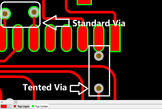
What is via?
A plated through hole (PTH) in a Printed Circuit Board that is used to provide electrical connection between a trace on one layer of the Printed Circuit Board to a trace on another layer. Since it is not used to mount component leads, it is generally a small hole and pad diameter.
Via Tenting
A via tenting is nothing but covering its annular copper ring with solder resist, also known as LPI (Liquid Photo Imageable) ink.
PCB designers need to remove solder mask pad from via location in their design, which comfortably enables QualiEco engineers to provide via tenting. This is why, it is considered as the easiest and absolutely FREE process. In this process, we can only ensure that the annular copper ring is covered with solder resist ink. The surface of the hole may or may not be covered with the solder resist ink.

Pros
No cost involved
Cons
Since via tenting is achieved by just removing solder mask pad from design, applying solder resist ink (LPI) may not cover the surface of the hole completely. If layer of LPI solder mask is broken over via hole, it provides a way for corrosive flux, moisture and other chemicals to enter. These impurities can finally be trapped, which increases the possibility of via failure as the corrosion starts eating plated copper inside the barrel.
With the popularity of No-Clean flux in SMT assembly these days, the possibility of contamination has been reduced significantly. However, corrosive Water-Clean flux still prevails in TH assembly and can cause problem. To tackle this issue, it is best to use any surface finish but HASL, which will reduce the risk at a greater extent.


