Peelable mask
Carbon
PTH on the Edge
Edge Plating
Countersink
Counterbore
Depth Routing
Press-fit holes
Single Side Double Access
Air Gap Structure
Peelable mask
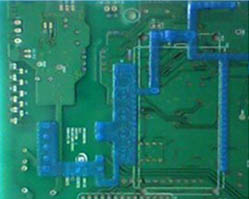
Peelable Solder Masks are applied by screen-printing, act as in-process protection (protection of selected board areas during the Surface Finish or Assembly Process to keep solder from flowing onto contacts, terminals and plated through holes (PTH) and are removed after processing at the assembler.
Process capability:
The peelable mask required single sided 6mil greater than the circuit pad, and it should be 16mil far away from the pad which is not required peelable mask.
 Notice:
The peelable mask is not suitable for the immersion tin, immersion silver, easily oxidized or scratched boards, because the peelable mask need a high temperature baking solidification.
Carbon
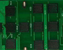
It is the use of screen printing technology, printing carbon ink on the PCB designated position, after high temperature baking solidification, it is having a certain resistance carbon film , usually used as a jumper, button, and through hole.
Process capability:
The carbon pad required single sided 4mil greater than the circuit pad, and it should be 10mil far away from the pad which is not required carbon, the spacing between carbon pad is ≥16mil
Notice:
1.We can not guarantee the resistance value of carbon
2. The carbon technology is not suitable for the immersion tin, immersion silver, easily oxidized or scratched boards, because the carbon need a high temperature baking solidification.
PTH on the Edge
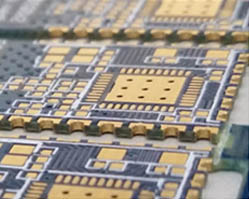
It is also called “castellated holes”. These are plated holes cut through on the board edge and used to join two PCBs either by direct soldering or via a connector. During the production, it is necessary to pre-process the semi-hole position before etching circuit to make sure the semi-hole position is smooth and no burr.
Process capability:
The hole diameter on the edge is minimum 0.6MM, and the half hole should be drilled inside the boards ≥0.3MM
 Notice:
The spacing between castellated holes should be greater than 0.55MM, or it will easily cause short circuit.
Edge Plating
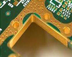
This means that most or part of the edge of a PCB or a cut-out is plated from the top side to the bottom side. This may be to ensure a good ground to a metal casing or for shielding purposes. To manufacture a board with round-edge plating we rout the board profile where the edge plating is required before the through-hole plating process.
Notice:
1.The edge plating location required at least 0.3MM circuit pad, or the copper will be easily peel off.
 2. As we need to hold the circuit within the production panel during processing we cannot plate round 100% of the edge. There must be some gaps (at least three gaps) so that we can place rout tabs.
Countersink
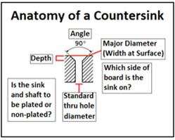
A countersink is a cone shaped hole cut into the laminate. It is typically used to allow the tapered head of a screw to sit flush with the top of the laminate. By comparison, a counterbore makes a flat-bottomed hole and its sides are drilled straight down. This is usually used to fit a hex-headed cap or screw.
To accurately drill your countersunk holes, we will need the following information.
1. Angle of the drill
2. Major Diameter (finished diameter of the hole at the surface)
3. Depth the countersink is to be drilled
4. On which side of the board is the sink? Top or Bottom?
5. The finished diameter of the shaft of the hole
6. Is the sink and shaft to be plated or non-plated?
Process capability:
The depth tolerance of the countersink hole is +/-0.15mm.
Notice:
1.Countersunk-head screws that follow the ISO standard very often have a 90° angle, if you require the other angle, we need to purchase the drilling tool.
2. The data of countersink hole is mutually restricted, so if you are changing one data, you should change the others accordingly.
Counterbore
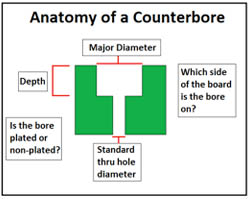
A counterbored hole is typically used when a fastener such as a bolt or cap head screw is required to sit flush with or below the level of a surface.
To fabricate your counterbored holes, we need to know the following information.
1. Major Diameter (finished diameter of the hole at the surface)
2. Depth the countersink is to be drilled
3. On which side of the board is the sink? Top or Bottom?
4. The finished diameter of the shaft of the hole
5. Is the bore and shaft to be plated or non-plated?
6. Because the sides of the hole are always parallel, there is no need to specify an angle.
 Process capability:
The depth tolerance of the step hole is +/-0.15mm.
Depth Routing
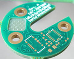
Normally all routing done on a PCB is going through the whole board thickness. PCB Depth control routing technology is the stepstair or groove shaped by partial routing in printed circuit boards(PCBs) manufaturing.It have great advantages in PCB assembly as the special shape of depth routing.
 Process capability:
The depth tolerance is +/-0.15MM; the minimum depth is 0.3 +/-0.15MM; the minimum balance thickness is 0.4+/-0.15MM
Press-fit holes

Press-fit holes are used as PTH holes to fit the leads of connectors that will not be soldered but pressed into the holes. The hole tolerance is tighter than the standard +/-0.075mm, usually it is +/-0.05mm, so even required +/-0.025mm.
 Process capability:
The tolerance of press-fit holes we can control is +/-0.05MM
Single Side Double Access
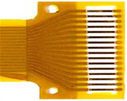
Applied with single sided material to make pattern but make some window on base film and add on cover layer on pattern top. The final products will have single layer copper but two side access possibility. This structure we call that single side double access boards.

Air Gap Structure
 The type of Air Gap Structure uses two single-sided flex circuits and applies pre-punched dynamic area adhesive in between to achieve high-flexible demand. It must pass through the process of CNC and plated through hole in advance to conduct the circuits on both sides then cover each single-sided flex circuits with a protective layer after the circuits were formed. It is able to design circuits on both sides and carry out plug-in and out, contact, lamination and soldering.
