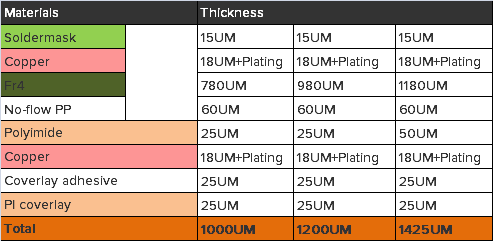
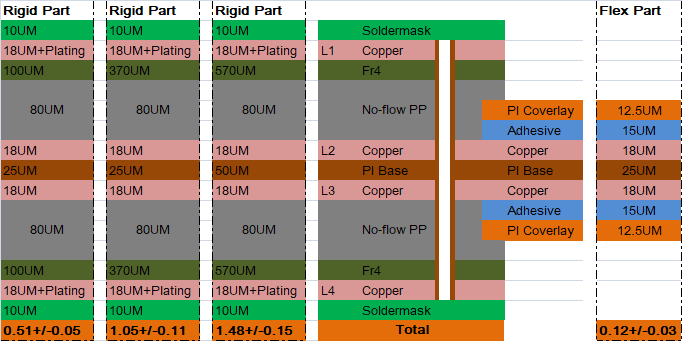
→Multilayer Rigid Pcb Stackup Design...
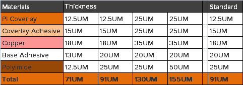
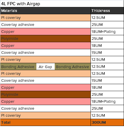
The standard layer buildups for Flexible pcb are as follows. Variations from these defaults are of course also possible, please contact us. We would be happy to provide you with in-depth consultation to determine the optimum solution.
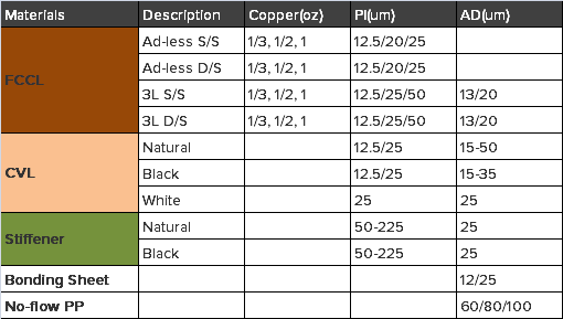
Commonly used materials specifications
A single sided flexible printed circuit construction with a polyimide cover film laminated to copper allowing access from one side only. One single conductive layer, either bonded between two insulating lamination or uncovered on one side.
Applied with single sided material to make pattern but make some window on base film and add on cover layer on pattern top. The final products will have single layer copper but two side access possibility. This structure we call that single side double access boards.
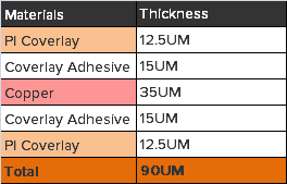
Double sided flexible circuit consist of double-sided copper clad material with top and bottom cover films (PI or Green/Yellow Oil, etc). Two conductive layers with an insulating layer between, plus convert layers on outer layer. The cover films are pre-routed to access copper from both sides using plated thru holes (PTH).
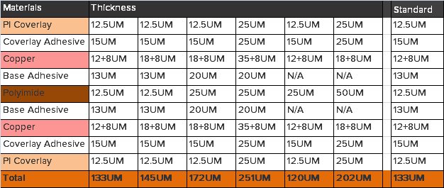
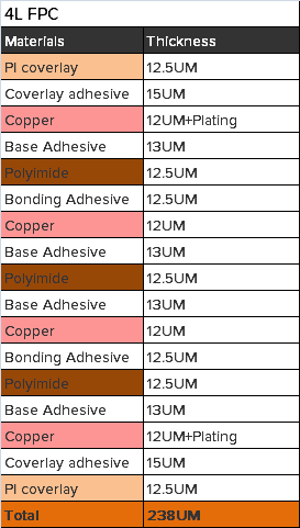
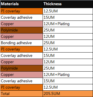
The structure of the multilayer flex board can be different combination of single-sided and double-sided PCB material , such as a 4 layer board that can be made of 2+2 or 1+1+1+1 , it also can be 1+2+1 (2 single-side PCB + 1 double-side ), the structure based on the actual situation.
Stiffeners are added to rigidize areas of a circuit to strain relieve component attachment locations, provide a firm surface for mounting, or increase thickness of the circuit to correspond to the mechanical specifications (e.g. ZIF connector).

The standard layer buildups for Rigid-Flex circuit boards are as follows. Variations from these defaults are of course also possible, please contact us. We would be happy to provide you with in-depth consultation to determine the optimum solution.
