Normally, there are 3 methods to dissipate the head for printed circuit board.
1. Utilize Thick Copper Traces
When you need a PCB for high-power applications, adding thick and heavy copper traces is usually the right choice. By utilizing thick copper traces, the heat will have a larger surface for heat distribution and dissipation.
2. Use Thermal Via Arrays

Thermal via arrays are another excellent choice for heat dissipation, helping to increase copper’s area and mass. By expanding the copper’s mass and area, a device will have reduced thermal resistance. Thermal via arrays also offer greater heat dissipation for critical components because they allow for better conduction. Due to their ability to dissipate heat and reduce thermal resistance, companies often utilize thermal via arrays close to heat sources to achieve improved performance.
Specification to holes:
i.Eight mils (0.2 mm) is the typical minimum mechanical drilling size. Twelve mils (0.3 mm) is more common and lower cost if the design will permit
ii.IPC-6012 specifies a minimum 20-µm (0.8-mil) copper plating thickness for a Class 2 PCB, but manufacturers target 25 µm (1 mil). As discussed earlier, the more copper thickness plated in the via, the iii.more heat can be transferred
PCB thickness may have an impact on the thermal via performance
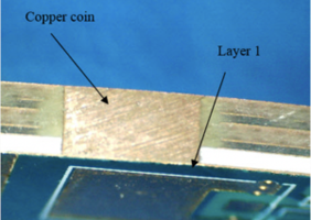
3. Cavtiy or routing zone embedded by copper coin

Copper coins are small pieces of copper embedded in the PCB. They’re usually placed directly under a component generating a lot of heat. They take advantage of copper’s superior heat conductivity to pull heat from the component straight to the heat sink. Copper coins are a great way to dissipate heat and are commonly used when you have a small number of components that generate most of the heat.
Specification to Copper coin:
Size: 3.000 X 3.00mm (min); 60.00 X 80.00mm(max).
Copper coin thickness: 1-3mm
PCB Surface finishing: ENIG(must be this).


